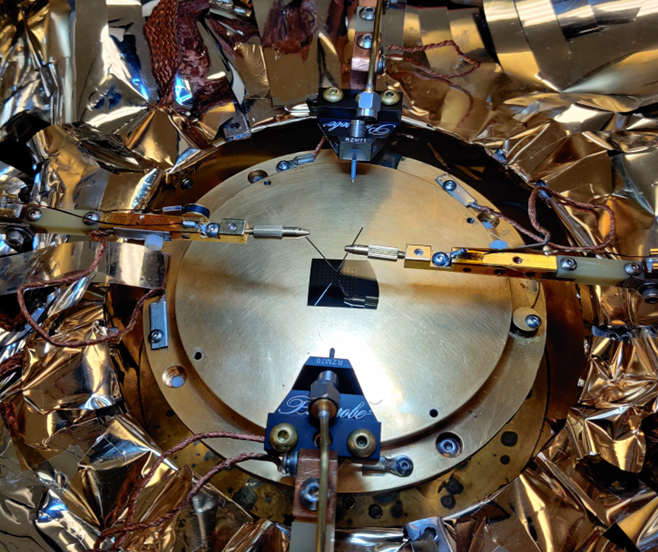
SuperFab, located at Royal Holloway, University of London, is the UK’s national facility for the development of superconducting quantum technology with a focus on quantum computing. Although a relatively new facility, it has already become central to the UK’s efforts to become a world-leader in quantum technology and commercialise quantum computing. NPL is working with the SuperFab team to establish best practice for characterising superconducting quantum devices.
SuperFab has state-of-the-art equipment for device fabrication, including thin-film deposition and e-beam lithography, however, there is a crucial bottleneck when developing state-of-the-art fabrication processes such as, when scaling from single qubit to large scale quantum processer, characterisation over many devices becomes crucial which involves gathering data about parameter spread and device variability. Our team has therefore procured and commissioned a new cryogenic probe station for automated on-wafer testing of superconducting circuits, which is has been installed at Royal Holloway. This will allow users to automatically, and with good repeatability, test many on-wafer devices at temperatures down to 4K. It can also be used for on-wafer testing of radio-frequency (RF) structures and components at frequencies up to 18 GHz.
Understanding the parameter non-uniformity across a wafer can help compensate for it in the fabrication methods. This is important for quantum computing companies looking to scale from single qubit to a large-scale processor. However, characterisation over such a large wafer can be extremely time-consuming and resource intensive. There is also a requirement for calibrated measurements which allow for verification and comparison of different designs, which can be difficult to achieve once a device is fully packaged. This is especially important for companies designing and manufacturing RF/microwave circuits such as superconducting quantum processors, or the RF electronics involved in calibration measurements.
Automated cryogenic probe station
 A cryogenic probe station is now available at the SuperFab facility of Royal Holloway, University of London for automated on-wafer DC testing of superconducting circuits for industry access. This will allow users interested in improving design, modelling and fabrication of multi-qubit quantum circuits to automatically, and with good repeatability, perform DC characterisation on large scale wafer at temperatures down to 4K using the in-built software. It can also be used for on-wafer testing of RF structures and components at frequencies up to 18 GHz which is useful in testing or characterising cryogenic electronics.
Using these new capabilities and learnings, we have developed an improved process for the design, modelling, and fabrication of multi-qubit quantum circuits. This is feeding into a roadmap for fabrication of multi-qubit circuits research and benchmarking. The ultimate goal is to support the fledgling industry and academic community with benchmarking and metrology by using this capability to develop metrological methods. focused on scalability of qubits and characterisation of RF/microwave circuits.
Would you like to speak to our quantum team?
Contact our quantum team